PRIVATE BETA — PCB Canvas is in TestFlight. Join the waitlist below for an invite.

PCB design finally feels modern.

Professional board design built for iPad, touch, and Apple Pencil. Place real parts, route real boards, verify your work, and send it to fabrication — without fighting desktop CAD.

KiCad in. KiCad out. No lock-in.
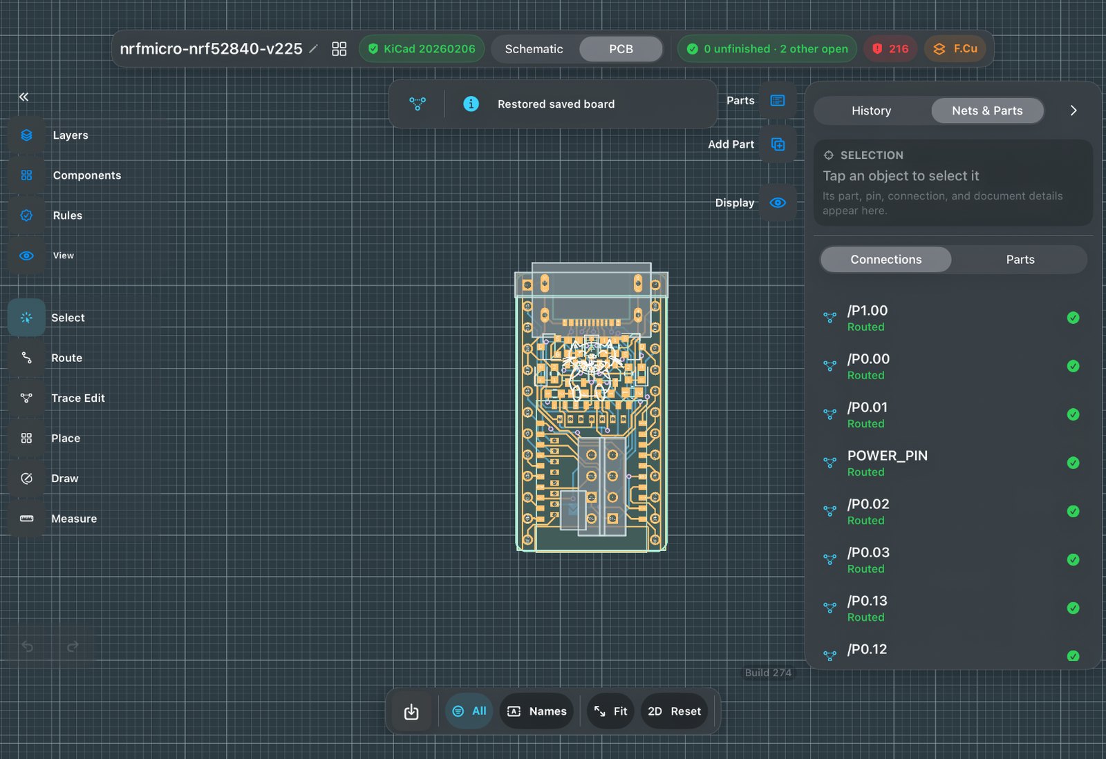
PCB Canvas editing an open-hardware nRF52840 board: routed copper on the canvas, net list with routed status, mode rail with Select, Route, Trace Edit, Place, Draw and Measure

The actual app — an open-hardware nRF52840 board, opened from its KiCad file, routed nets and live rule checking on screen.
Design naturally

The board is the workspace.

Direct manipulation on the canvas itself — not dialogs about the canvas. Selection, placement, routing, and editing all happen where your hands already are.

Route where you want it to go.Tap intent points with the Pencil; the router refines instead of refusing. Tap back to undo a bad leg.

Move the part. The traces clean themselves up.Clean Move reconnects routing into a result that looks intentional.

Tap the wire you meant.Copper-first selection: a trace crossing a part body wins the tap, and the whole net lights up.

Exact when you need exact.Type a coordinate, work in mm or mils, snap to a real grid. Precision is a tap away, not a mode away.


Let the tool do the tedious work

It does the part of PCB design you never wanted to do.

The recurring difference isn’t prettier commands — it’s work you simply don’t do anymore.

Place the MCU. Get the circuitry it needs.Decoupling caps, crystal, pull-ups, balun — offered pin-bound and placed at valid pads. Antennas are asked about per board, never assumed.

See the footprint before you place it.Function-first catalog with real manufacturer part numbers and inspectable land patterns — and pads you can edit, add, or draw straight onto the board.

Missing part? Feed it the datasheet.BETALand patterns derived from the PDF’s vector geometry — instead of you transcribing the drawing pad by pad.

Say what the copper should be, not how.Stackup with impedance targets expressed as intent; routing rules follow the net class.


Know what you're building

Confidence is a feature.

A workflow isn’t done because the final button exists. Discover → inspect → decide → act → verify — the product is built around that standard, and where it isn’t met yet, it says so.

Inspect real geometry.Actual footprints, actual clearances, integer-nanometre coordinates displayed in your units.

The router tells you why, not just no.Blocked routes explain themselves and offer to make room.

Rules that ride along.Net classes, clearance, and manufacturing rules live in the workspace rail.

Board-wide DRC, live.Ambient checking with a problems surface, reading your board’s own design rules. Six rule families verified item-for-item against KiCad 10 — clearance, board-edge, courtyard, annular ring, mask bridge, silk height.


Send it

From board to board house without a plot dialog.

Export asks what you’re ordering — not which of eleven file formats you’d like to configure.

Know what you’re sending to the board house.One validated zip: Gerbers, drill files, BOM, and pick-and-place. Geometry is checked before a single file is written.

Stale copper never ships.If a pour is out of date, export refuses and names it — it will not silently rewrite your board.

Part numbers included.The BOM carries LCSC part numbers, ready for assembly quoting.

And it’s still a KiCad board.Everything you export opens in desktop KiCad, because it never stopped being a .kicad_pcb.

PCB Canvas Labs PROTOTYPE

Make the board the art.

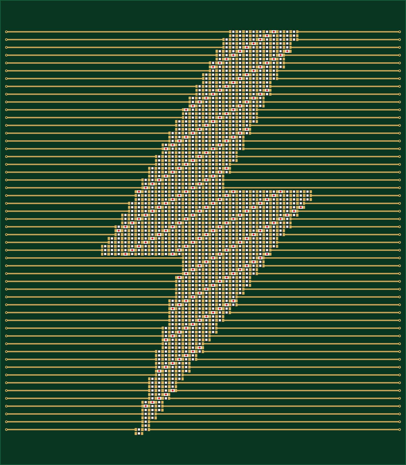
Upload a logo. Get back a legal board where every dark pixel is a real, orderable component — this bolt is 1,189 actual parts (1,022 resistors, 167 red LEDs), daisy-chained with 1,293 real copper traces, escaping to vias at the board edge. Not a silkscreen print: nets, pads, drills, and an LCSC-numbered BOM.

A lightning bolt rendered as 1,189 real 0603 components on a green PCB, with traces fanning in from both board edges

A working lab experiment, not yet in the product — shown because it's exactly the kind of thing the engine underneath makes possible.

The promise

Your boards are yours.

No account needed to design. Install, open a board, start working. Sign in only when you want cloud services.
Cancelling can’t take your work. Local boards stay editable and exportable regardless of subscription state.
Standard files, always. Your design is KiCad data end to end — portable to the desktop at any moment.
Offline is normal. Core editing works with no network; paid features ride out outages on a cached entitlement.
Honesty section

Where KiCad still wins.

You’re an engineer; you’d find out anyway. This list is generated from our own capability audits, and shipping features off it is part of the roadmap.

Watch this list shrink. When a gap closes, its row comes off — that’s the deal.

  • Silkscreen rules, and rules that compare against a library. Board-wide DRC runs live here, and six rule families match KiCad item-for-item by UUID — clearance, board-edge clearance, courtyard overlap, annular ring, solder-mask bridge and silk text height. One honest caveat: KiCad keeps design rules in the project file, so we read your .kicad_pro when it’s available; where a threshold is still our default rather than your rule, the finding says so in as many words. Two families are still open: rules that measure the extents of rendered TEXT sit on a stroke-font glyph model we shipped in build 285 (the author’s CC0 newstroke data) — the rules on top of it are next, and rules that compare a footprint against its source library need a library binding that a single-file editor doesn’t have.
  • 3D viewing. KiCad has a native 3D viewer. We export STEP for fit-testing but don’t render the board in 3D on device yet.
  • Updating a footprint from its library. You can draw, edit, add and remove pads here, and swap a footprint for another from the catalog. What you can’t do is re-pull a footprint from the project library it came from — most real boards use project-local libraries, and refreshing from ours would quietly substitute a different vendor’s land pattern.
  • Fabrication drawings. We write Gerber, drill, BOM and placement files. We don’t yet produce the PDF drawing sheet some fabricators and assembly houses ask for alongside them.
Pricing

Free gets you to a real, manufactured board. $5 removes the limits.

Free is the real editor — real routing, real rules, real precision, full KiCad compatibility. Nothing about your PCB is ever made worse because you're not paying. The limits are about scale and convenience, and they're honest ones.

Free

$0
learn it, build it, order it
  • The full editor, uncrippled
  • 2 active boards, swap anytime
  • 3 fab exports per month
  • KiCad in & out, offline
  • No account needed
Get early access

Plus

$5/mo
for people who kept using it
  • Unlimited active boards
  • Unlimited fab exports
  • Footprint extraction allowance
  • Richer catalog tools
  • Cloud sync & backup
Get early access

Pro

$12/mo
for heavy & advanced use
  • Plus, with bigger allowances
  • Cloud STEP / 3D services
  • Priority server processing
  • Priority support
Get early access

What we never paywall: DRC correctness, routing legality, precision, units, layer count, file integrity, KiCad compatibility, or access to your own files. If you stop paying, you fall back to Free gracefully — every board is preserved, you pick which two stay active, and everything stays exportable. Subscription state controls convenience and services, never ownership.

Draft pricing, pending approval. Subscriptions are not live — the app is pre-release. Paid features ride out network or billing outages on a cached entitlement; the editor itself never needed a connection in the first place.

Be first on the board.

PCB Canvas is in private development. Leave your email and you’ll be first in line for the beta.

DRAFT: waitlist backend not deployed. No data is collected by this preview page.