Build a Bluetooth speaker board
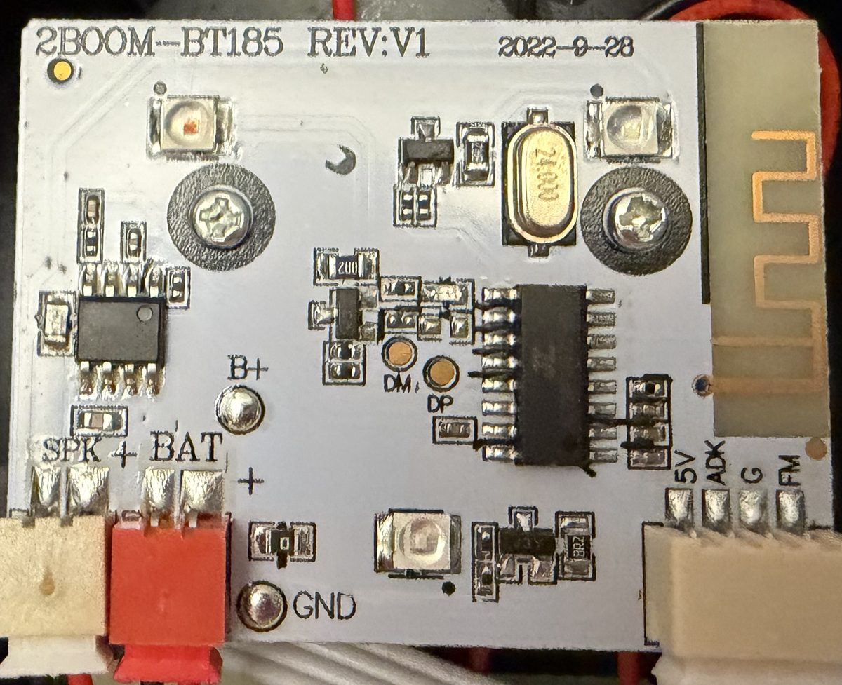
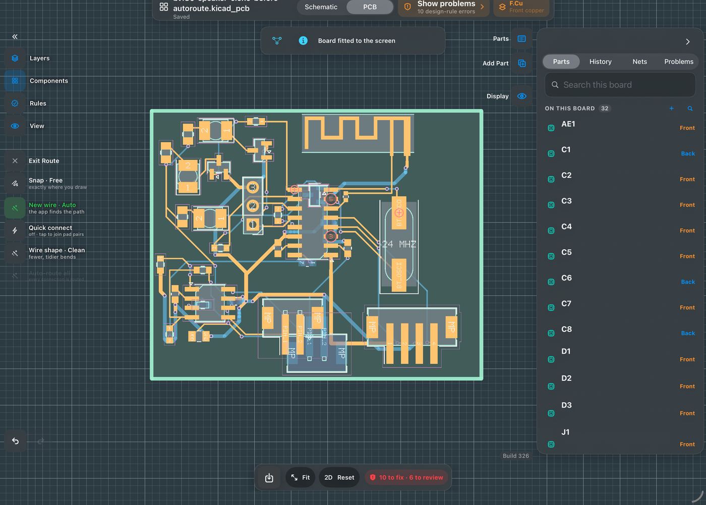
The little board inside a cheap Bluetooth speaker: a Jieli Bluetooth audio chip, a 3 W amplifier, a printed antenna, a battery and three LEDs. We photographed one (the 2BOOM-BT185), worked out every part, and rebuilt it in PCB Canvas.
What the board does
A phone streams music over Bluetooth to the Jieli chip. The chip decodes it and plays it out of one audio pin (DACL). A capacitor carries that signal to the amplifier, which drives the speaker. One Li-ion cell powers everything directly, and the Jieli chip charges that cell itself from the 5 V pin of the 4-pin connector. There is no separate charger chip.
What’s on the original
Read off the photographs. Jieli prints a lot code on its chips, not the part number, so the chip’s identity is worked out rather than read.
| Marking | Part | Package | Role | How sure |
|---|---|---|---|---|
JL AC23BP1X622-69D4 | Jieli AC6969D, 4 Mbit flash (AC6969D4, LCSC C22440788) | SOP-16 | Bluetooth 5.1 audio chip | High. Jieli marks the year and lot before the dash and the part after it (kagaimiq’s marking notes: -65A4 is AC6965A, 4 Mbit). 69D4 reads AC6969D with 4 Mbit; the AC6969 family is SOP-16, and LCSC sells it as AC6969D4 and AC6969A2. The board’s 5V, ADK, FM and DM/DP pads land on the AC6969D’s charger, ADC, FM and USB pins. No teardown we found names this exact marking. |
24.000 | 24 MHz crystal | HC-49/SMD | Chip clock | High (marking; Jieli reference design) |
8002D XS2348B | 8002-family 3 W mono amplifier, maker unknown. Same pinout as the NS8002 (LCSC C189960) | SOP-8 | Speaker driver | Pinout high (every 8002 shares it); maker not identified |
473 | 47 kΩ resistor beside the amp | Chip resistor | Probably the amp’s feedback resistor (sets the gain) | Medium: position only, not traced |
J3Y ×3 | S8050 NPN transistor (LCSC C2146) | SOT-23 | LED switches | High (standard marking) |
8R2 ×3 | 8.2 Ω resistor | Chip resistor | LED current limit, one per LED | High |
| (no marking) | LED ×3 | PLCC-2, about 3.5 × 3 mm | Light show | High |
| (meander trace) | Printed inverted-F antenna | Copper on the board edge | 2.4 GHz antenna | High |
| (no marking) | Small 2-terminal part beside BAT | SOD/SOT, tiny | Unknown: maybe a diode or protection part | Low: not identified, left off the clone |
| SPK, BAT, 5V/ADK/G/FM | 2.00 mm connectors (JST PH style) | 2-pin, 2-pin, 4-pin | Speaker, cell, lead to the button board | High (pitch measured from the photos) |
| DM, DP, B+, GND | Test pads | Round pads | USB data for flashing; battery and ground | High |
The AC6969D’s pin table is from Jieli’s own datasheet (V1.0, 2020-06-01, Table 1-1, via a distributor’s copy). Its part values are from Jieli’s reference schematic. Neither is a full English datasheet with layout guidance; Jieli does not publish one.
Parts you add
Two searches in Add Part. Everything else comes with them.
| Search for | Role | What the app adds |
|---|---|---|
NS8002 | Amplifier (U1) | 100 nF and 10 µF on VDD; 1 µF bypass capacitor; 20 kΩ input and feedback resistors; the +IN-to-BYPASS link; a 100 kΩ pull-down that keeps it on; the speaker connector |
AC6969D | Bluetooth audio chip (U2) | 1 µF on VBAT, VDDIO and VCOM; the 24 MHz HC-49/SMD crystal (no load capacitors: they are inside the chip); 2.7 pF to the antenna; the antenna you choose; 100 nF from the audio output; the battery connector; the 4-pin 5V/ADK/G/FM connector; DP/DM/GND pads; three LED channels (S8050, 1 kΩ, LED, 8.2 Ω) |
Steps
- New board
Boards ▸ New Board. Tap Width and type 45, tap Height and type 35, leave it on two layers, then Create Board. That is the original’s size.
- Add the amplifier
Add Part ▸ search
NS8002and take the top result. Put it at the lower left, where the speaker lead comes in: tap X beside the part and type 8, tap Y and type 26 (mm), or drag it there. Its offer lists eight parts and all eight start ticked, the speaker connector included, because it carries the audio out. The Feedback Resistor menu sets the volume: 20 kΩ is the datasheet’s value (gain 2), 47 kΩ is what the BT185 fits (gain 4.7, louder, clips sooner on a flat cell). Tap Place All. - Add the Bluetooth chip, turned round
Add Part ▸
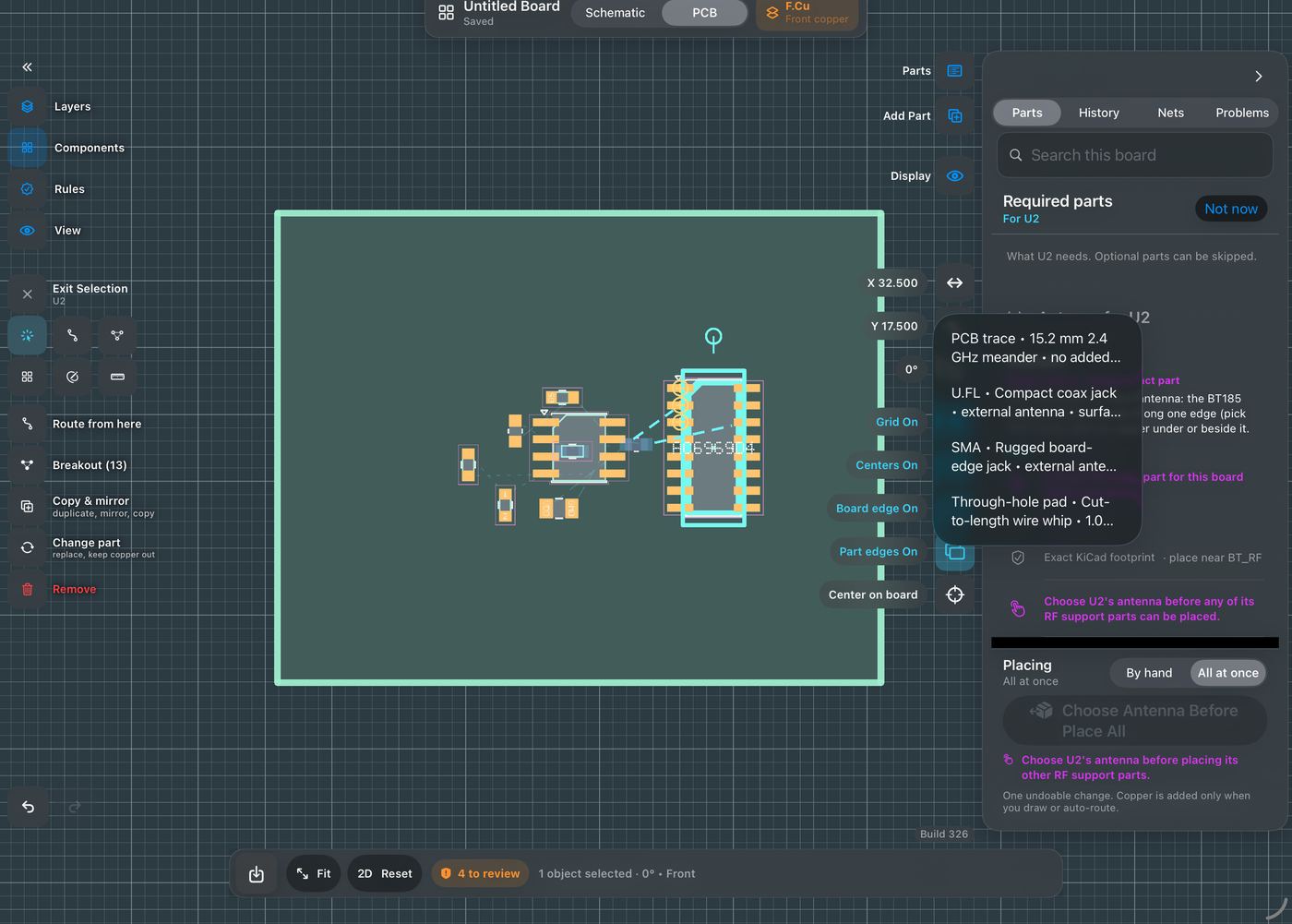
AC6969D▸ top result. While it is still in your hand, tap Turn 90° twice (beside Place), so pins 1–8 face the right edge: those are the battery, 3.3 V, buttons, FM, antenna and crystal pins, and the right edge is where the antenna goes. Then Place it and type X 22, Y 15 mm, a little left of centre and above the middle. (Once it has landed, the angle beside X and Y turns it too.) - Choose the antenna and battery polarity
The chip’s offer asks for the antenna and will not Place All until you answer: open the Antenna menu and pick PCB trace, the printed meander the BT185 uses. On the Battery Connector, pick BAT+ on pad 1 or pad 2 to match your cell. The required parts, the battery connector and the Connector (the 5V/ADK/G/FM lead, which brings in the 5 V) start ticked. The USB pads and the three LED Driver rows are yours to choose: open More and turn on Include in Place All for each one you want (each LED driver brings its resistor, LED and 8.2 Ω with it). Tap Place All. The antenna goes down first, on the board edge with its keep-out; then the 1 µF caps, the crystal, the 2.7 pF feed, the connectors, the USB pads and the three LED channels. The board grows from 35 to about 36.5 mm tall to fit them.
- Check the wiring (nothing to draw)
The two chips join by name. The chip’s VBAT, the amplifier’s VDD and the three LED resistors share
BAT; the chip’s audio capacitor and the amplifier’s input resistor shareAUDIO_IN; every ground isGND. Tap any pad to see its net. If Place All left a part out, its reason is in the offer’s result line. - Auto-route
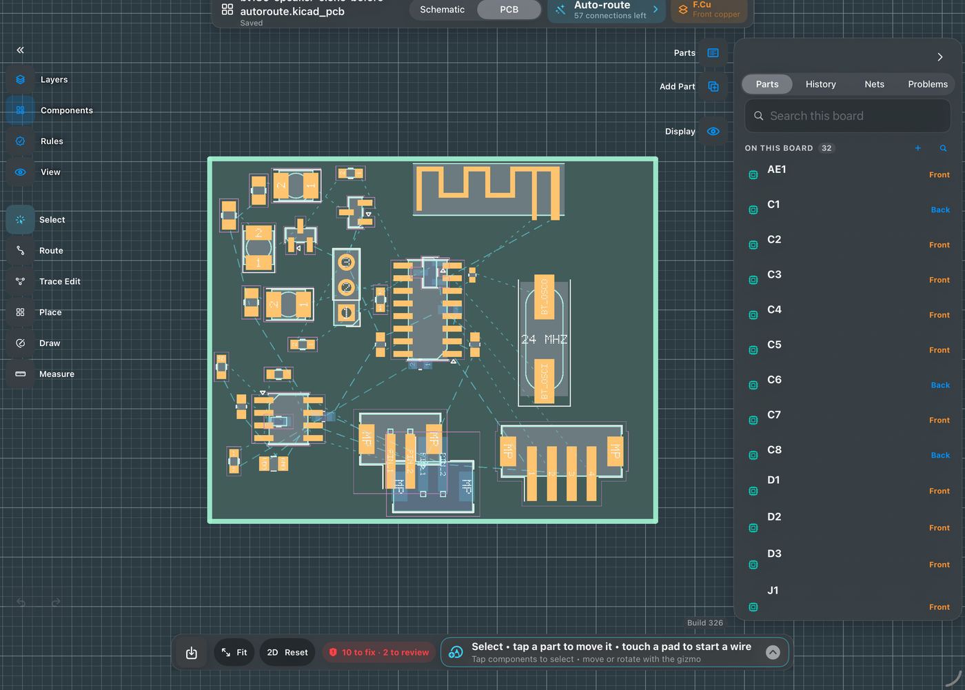
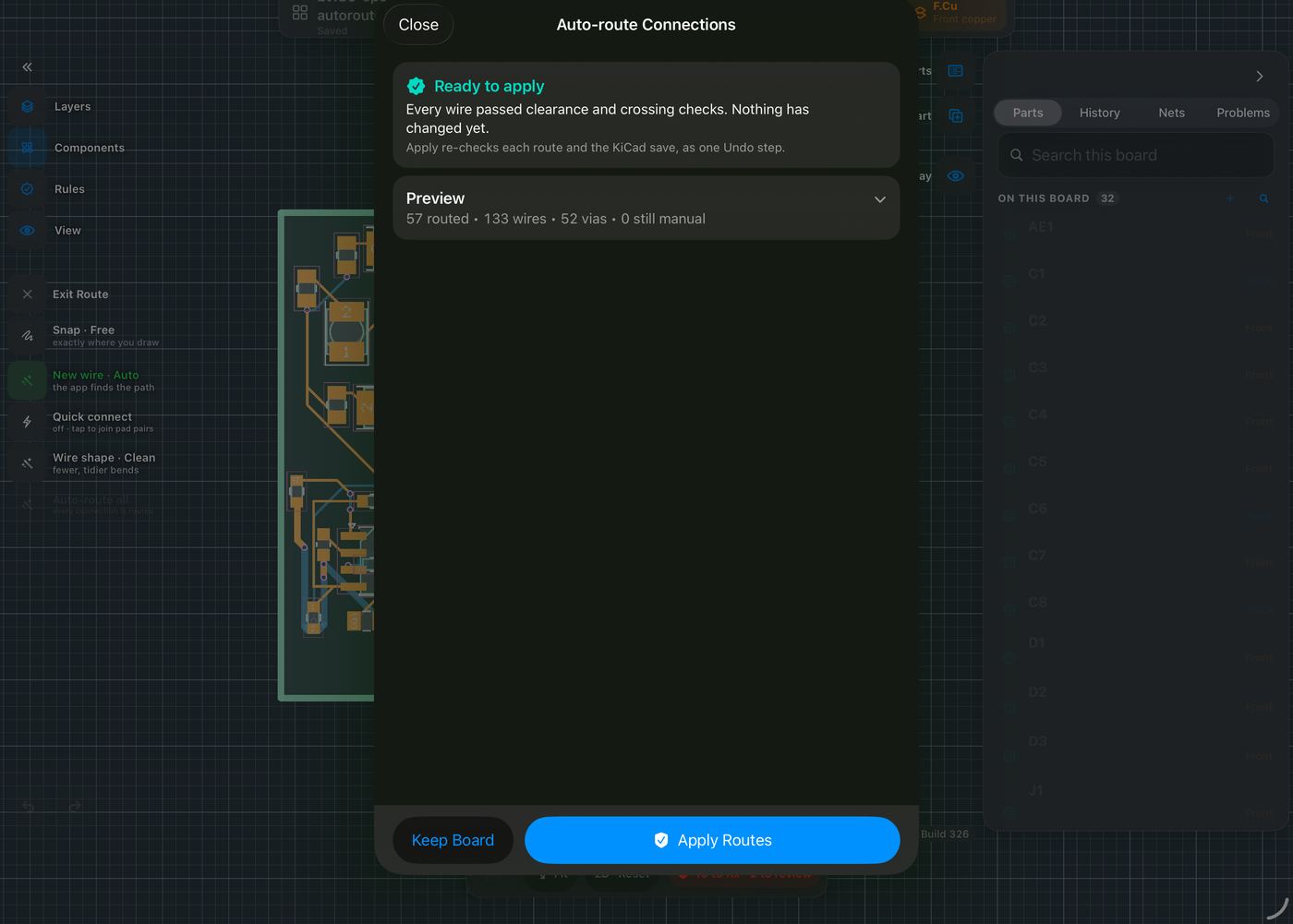
Route ▸ Auto-route all, then Apply. On this board it routes all 57 connections on two layers and keeps every trace out of the antenna keep-out.
- Check and export
Open Problems: anything blocking sits under “to fix” with a plain reason. Then Boards ▸ Export for Manufacturing ▸ Generate for Gerbers, and Export a Copy for the .kicad_pcb. KiCad’s own design-rule check passes on our reference build of this board (no errors; a few silkscreen-overlap warnings).
Pin reference
The AC6969D, from Jieli’s datasheet Table 1-1. Pins with two functions are named by the one this board uses; the other is in brackets.
| Pin | Name | On this board |
|---|---|---|
| 1 | LDO_IN (PB5) | 5 V in from the 4-pin lead: the built-in Li-ion charger (4.5–5.5 V in, charges to 4.2 V, up to 300 mA) |
| 2 | VBAT | The cell, 2.2–5.5 V. 1 µF |
| 3 | VDDIO | The chip’s own 3.3 V output. 1 µF |
| 4 | PB1 (ADC5) | ADK: the buttons, a resistor ladder on the other board |
| 5 | FMIP | FM: the lead itself is the FM antenna |
| 6 | BT_RF | 2.7 pF, then the antenna |
| 7, 8 | BT_OSCI, BT_OSCO | 24 MHz crystal (the table spells them BT_SOCI/BT_SOCO) |
| 9 | PC5 | LED 2 |
| 10 | PC4 (PWM1) | LED 1 |
| 11 | USBDM (PC3) | DM pad |
| 12 | USBDP (PA4) | DP pad |
| 13 | PA1 (MIC, PWM4) / PA0 | LED 3 |
| 14 | VSSIO | Ground |
| 15 | VCOM | Audio reference. 1 µF |
| 16 | DACL | Audio out, through 100 nF to the amplifier |
Before you order
- Antenna keep-out. Nothing but the antenna may sit in its keep-out: no parts, no traces, no ground fill, on either side. PCB Canvas places the antenna on the board edge with its keep-out and keeps routing out of it. Put the board in its case with the antenna away from the battery and the speaker magnet.
- Battery polarity. On the battery connector, choose BAT+ on pad 1 or pad 2 to match your cell’s red lead, then check it with a meter before plugging in. A reversed cell destroys the chip. Use a cell with its own protection board: nothing on this board cuts off a shorted or flat cell.
- Speaker wiring. The amplifier is bridge-tied: both speaker wires carry signal, and neither may touch ground or the case. Use a 4 Ω or larger speaker. Swapping the two wires only flips the cone’s phase.
- Amplifier heat. Into 4 Ω from a full cell the 8002 dissipates up to about 0.9 W, and the SOP-8 is rated 140 °C/W to air. Give its pins generous copper and keep the volume sensible, or use an 8 Ω speaker.
- LED current. 8.2 Ω from a 4.2 V cell lets about 140 mA through an LED. The original’s firmware pulses them; for steady LEDs fit 47–100 Ω.
- Charging. The chip charges at up to 300 mA from 5 V on pin 1 of the 4-pin lead. A cell rated below 300 mA needs the firmware to set a lower current.
Firmware
A blank AC6969D does nothing. Jieli’s chips run Jieli’s firmware, and the tools are closed:
- Buying the chip pre-flashed is how speaker makers do it: the seller loads a stock “Bluetooth speaker” image. Ask your supplier for one with the button ladder, LED and battery behaviour you want.
- Flashing it yourself uses the DP and DM pads (USB) with Jieli’s Windows download tool and an SDK image. The SDK and tools reach customers through Jieli’s distributors, mostly in Chinese, and need an agreement.
- Open tools exist from the community, for example kagaimiq’s jielie notes, which document the chips and their USB loader. They are reverse-engineered and unofficial; nobody publishes an open speaker firmware for this chip that we know of.
So plan to order chips already flashed, or budget time for Jieli’s toolchain. PCB Canvas makes the board; it cannot make the firmware.
If Place All rearranges things
On a board this tight Place All may turn the chip, move it to a roomier spot, push a part to the back or grow the board so that every part fits within the distance it needs. It never does so silently: the result under Place All lists each change (“turned U2 90° and moved it 6.0 mm so every part it needs fits”, “C5, C6 placed on the back, under the pins they serve, to fit… that distance is electrical”, “board grew to 45.0 × 38.5 mm”). One Undo puts it all back. If you want one-sided assembly, move the back-side parts to the front and let the board grow; a decoupling capacitor further than 2 mm from its pin stops decoupling, so keep it close.
What the app can’t do yet
- One antenna shape. The only printed 2.4 GHz antenna on offer is a reviewed 15.2 mm meander (TI AN043 / SparkFun), not the BT185’s own trace. It is a proven design but untuned for this board and case; the 2.7 pF feed capacitor is Jieli’s reference value. Tuning needs a network analyser.
- Connector style. The original’s connectors enter from the side; the catalogue has top-entry 2.00 mm JST PH footprints, so those are what the clone uses.
- Two parts left as the original’s mystery. The tiny two-terminal part beside BAT is not identified and is not on the clone. The 47 kΩ beside the amplifier is offered as a gain choice, but its position was read from a photo, not traced.
- Muting the amplifier from the chip (the 8002’s SD pin on a GPIO) is a connection you draw yourself; the clone holds the amplifier on.
- The Jieli chip has no KiCad symbol. Its pins come from Jieli’s datasheet table and are typed by hand; the land pattern is the standard SOIC-16 chosen from the datasheet’s package drawing.
- No firmware. See above: the board is complete, the software is Jieli’s.