Know the workspace
If you’ve never designed a circuit board, start here. Ten minutes of orientation, no steps to follow. Every picture is the real app.
What a PCB is
A printed circuit board is a sandwich of fiberglass and copper. Parts (chips, resistors, connectors) sit on it. Each part’s metal contact patches are its pads. Pads that must be electrically joined belong to the same net, and the copper lines that join them are traces. You design the board, send files to a factory, and get boards in the mail. PCB Canvas is the design step, on an iPad.
The workspace
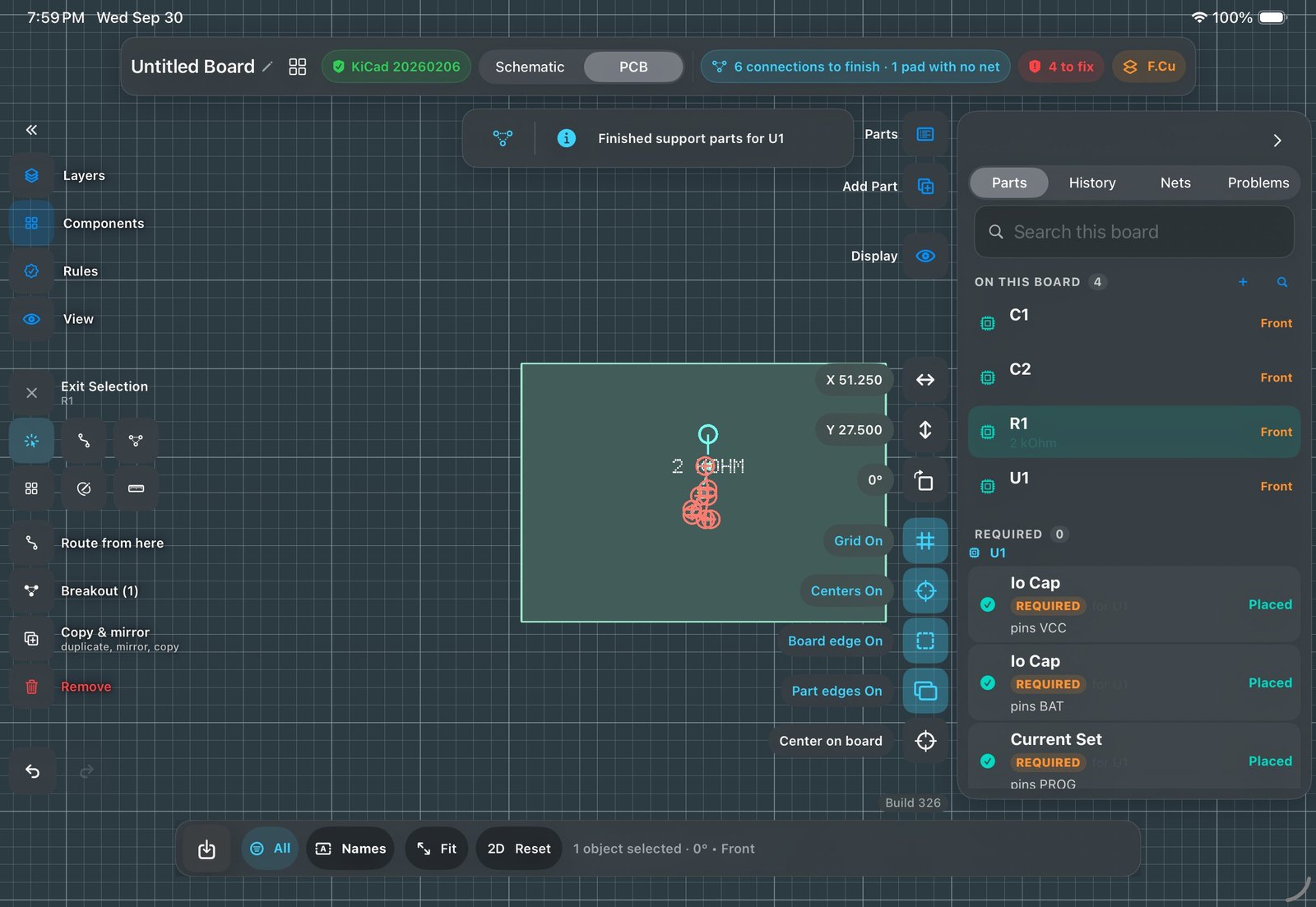 1
2
3
4
5
Parts arrive with their circuit
Chips rarely work alone. Nearly every one needs small companion parts, mostly capacitors and resistors, wired to specific pins. Datasheets call this the support circuit, and in most tools you build it by hand. Here, placing a chip offers its support circuit: each required part named, bound to the right pins, placed with one tap. Where real designs disagree, the app shows the options with counts from real boards and lets you pick.
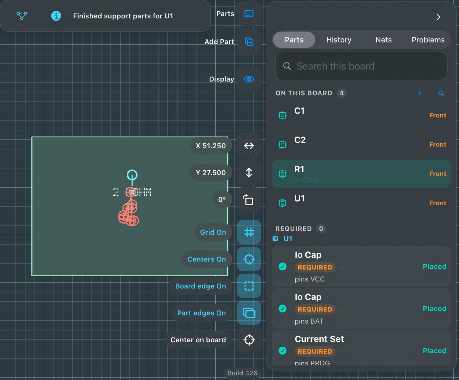
Routing
Connections that don’t exist yet show as thin guide lines, called the ratsnest. You make them real in Route: drag copper with a finger or the Pencil, or let Auto-route propose copper for everything left and apply it in one tap. The router moves other traces out of the way rather than refusing, and the status bar counts down the remaining connections.
Design rule checking
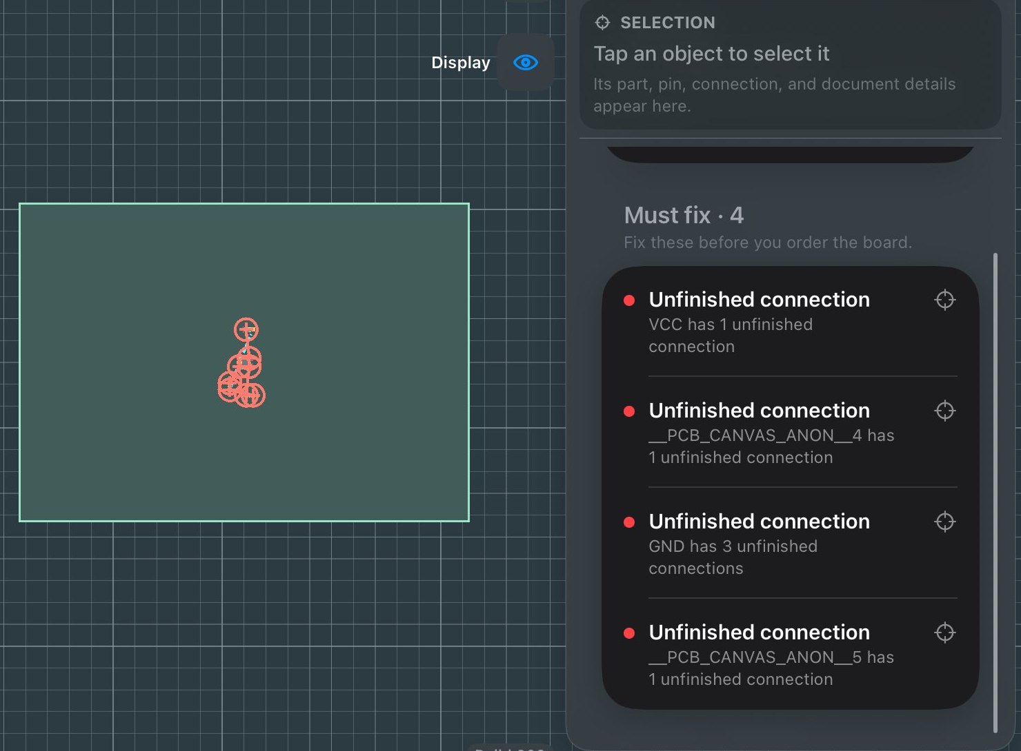
Design rules cover how close copper may get, how wide traces must be, and what a factory can drill. The app checks them continuously while you work. The Problems panel names each issue in plain words, with a button that moves the view to it. Findings never block you from working; they stay visible until fixed or accepted.
What you get out
Two things, both industry standard. A KiCad file, the open desktop EDA format, so the design is portable. And a manufacturing package: Gerbers (the copper artwork, one file per layer), drill files, a parts list, and placement coordinates. Both are generated and verified on the iPad and can be uploaded to a board factory as-is.
Terms the guides use
| Word | Meaning |
|---|---|
footprint | The pattern of pads a part needs on the board, its physical landing site. |
net | A named set of pads that must all be connected (GND, VCC, …). |
via | A plated hole that carries a trace from one copper layer to another. |
pour | A filled copper region, usually ground, flooding the spare space. |
DRC | Design-rule check, the continuous inspection behind the Problems panel. |
Gerber | The file format factories read; one per copper/silk/mask layer. |