A tiny Li-ion charger
Your first board: a TP4054 lithium charger, about the size of a postage stamp. One chip, its required components, a few routed connections, and an export. It covers every stage you’ll use on bigger boards.
What you’re building
Charging a lithium cell safely means two phases: a controlled constant current until the cell nears 4.2 V, then a constant voltage hold while the current tapers. Getting that wrong ruins cells, so the standard approach is a charger IC with the sequence built in. The TP4054 is a common small one: five pins, no external transistors, one resistor to set the charge current.
You place that one chip and PCB Canvas offers the components it requires, placed and bound to the right pins. Every number and screenshot below comes from a run of these steps on the beta. The run took about five minutes end to end.
Steps
- New board
Boards ▸ New Board ▸ width
30▸ height20▸ Create.Why these numbers: 30 × 20 mm gives one chip and its companions room to route. Two copper layers, the default, puts traces on top and leaves the bottom free for crossings and a ground pour later. More layers help on dense boards; this one doesn’t need them. - Add the charger
Add Part ▸ search
TP4054▸ take the top result ▸ tap the board to place it. It lands as U1 with 5 pads.The five pads: power in (VCC), cell out (BAT), ground, a charge-status pin, andPROG, which sets the charge current. Everything else on this board serves those five pads. - Take the support offer
Tap Place All. Three parts arrive. Here is the list it shows, and what each row actually is:
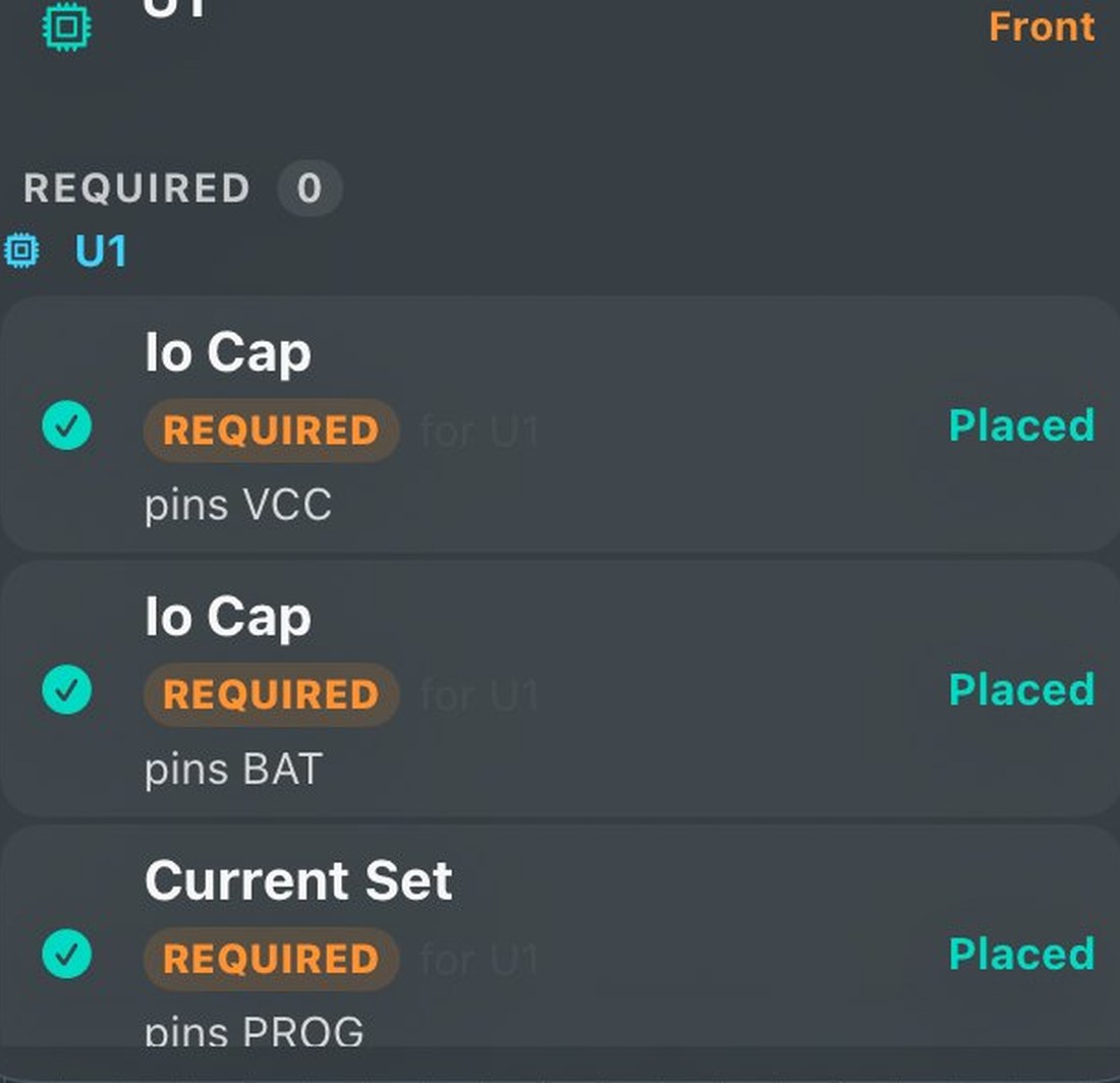
Each REQUIRED row names the pins it serves and reads Placed. “Io Cap · pins VCC” is C1, “Io Cap · pins BAT” is C2, “Current Set · pins PROG” is R1. What those parts do. C1 (input cap): wires and batteries have some inductance, so when the charger suddenly draws current the input voltage dips. A capacitor atVCCrides out the dips. C2 (battery cap): the chip’s control loop needs a capacitor onBATto stay stable. The datasheet requires it, so the app places it. R1 (2 kΩ onPROG): the chip holds about 1 V across this resistor and mirrors that current times 1000 into the cell, so 2 kΩ gives roughly 500 mA of charge current. For a small cell, use a larger resistor: 5 kΩ gives about 200 mA. Choosing that one value is the main design decision on this board.And the suggestion underneath: the offer also proposes a USB-to-UART bridge, “on 9 of 18 projects using TP4054.” That number is mined from real open-hardware boards. Suggestions carry their evidence and are never ticked for you. - Read Problems
Open the right panel ▸ Problems. Four rows:
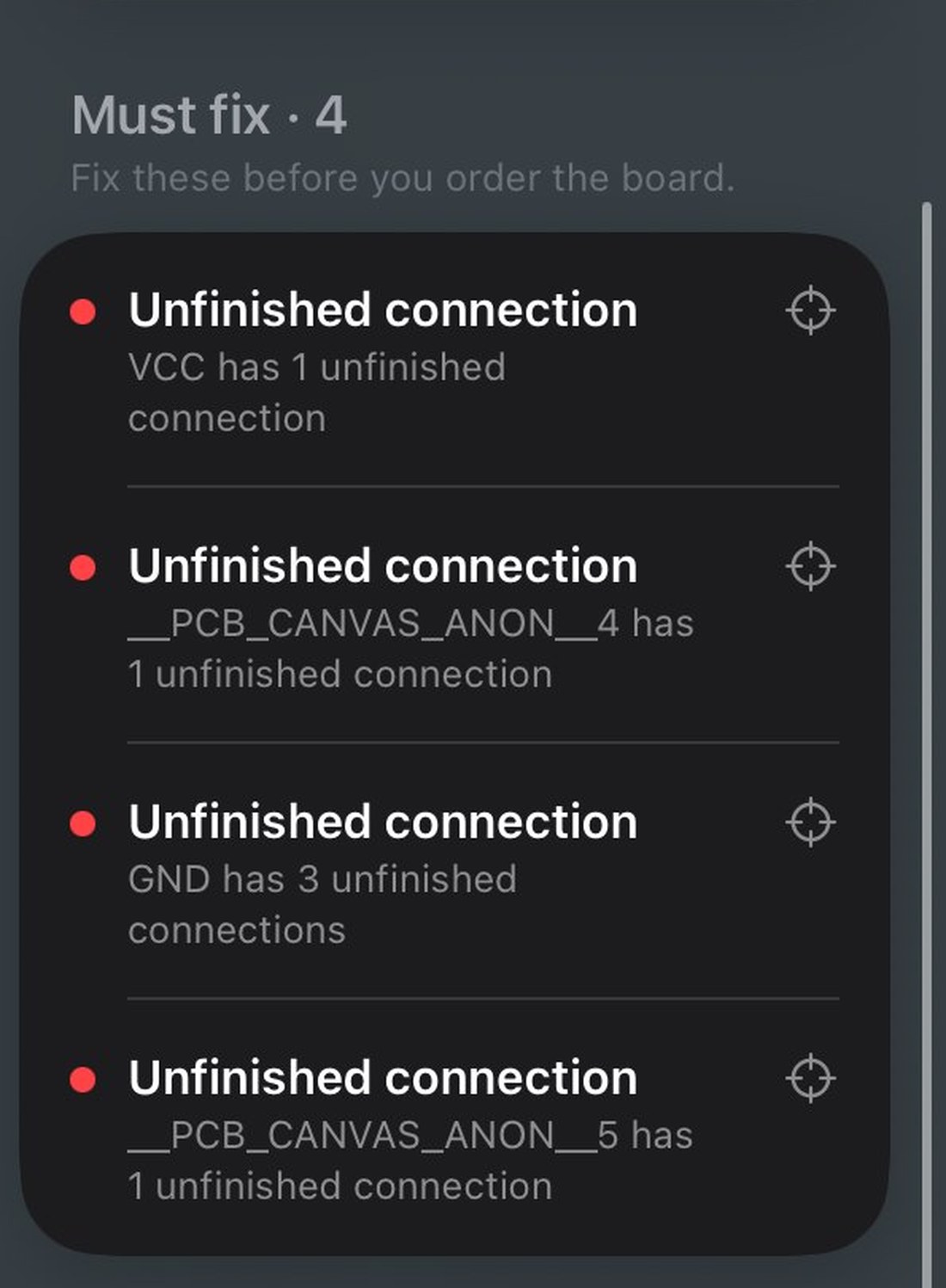
“VCC has 1 unfinished connection” means C1 isn’t joined to the chip’s VCC pad yet. “GND has 3” means three parts still need a path to ground. The two __PCB_CANVAS_ANON__rows are connections nobody named: C2 to BAT and R1 to PROG exist electrically, so the app names them automatically.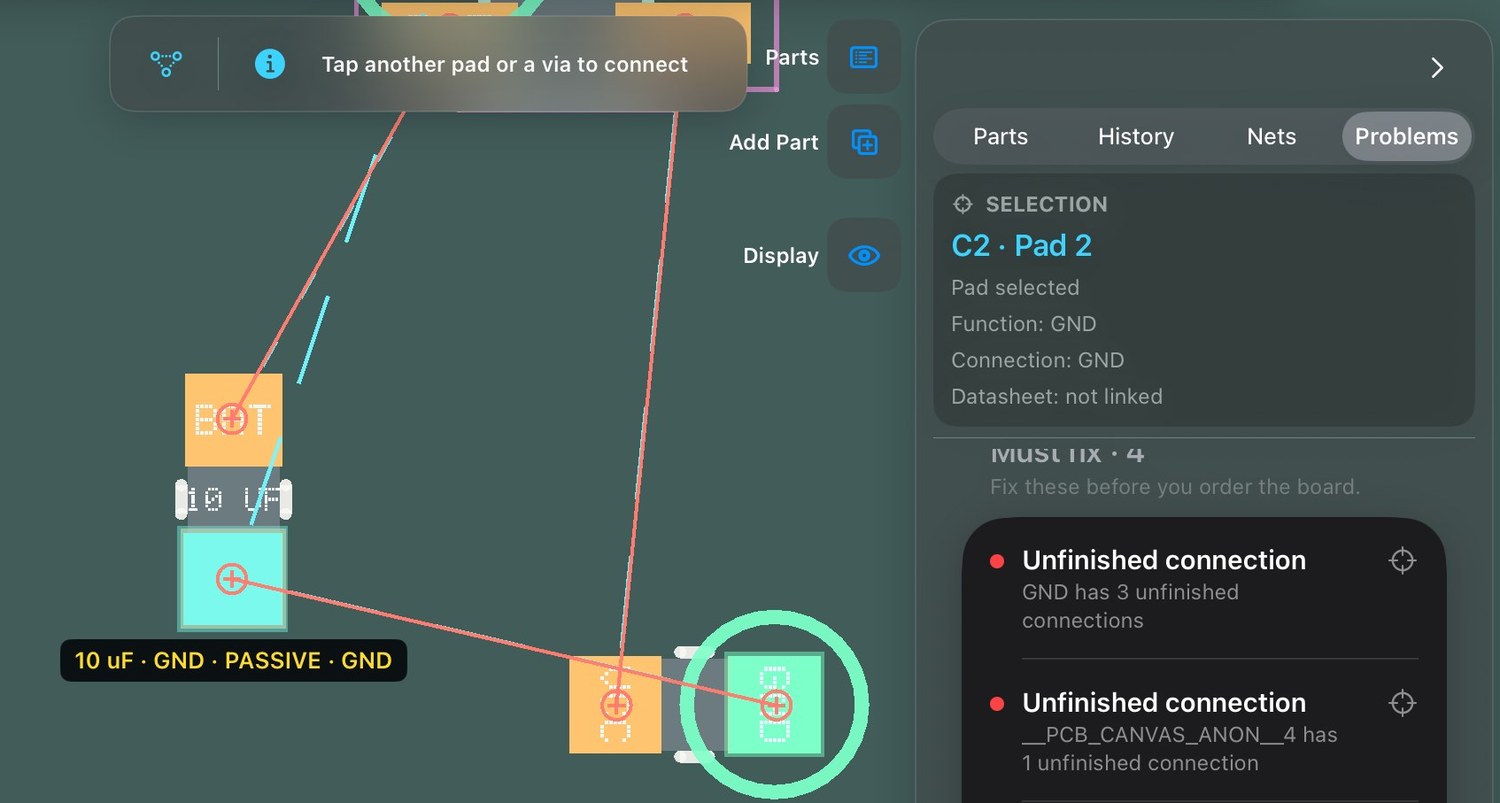
After tapping a problem row: the canvas zooms to the part, rings the pad, and the selection card confirms what is selected. Here that’s C2, pad 2, function GND. At this zoom the capacitors show their 10 µF markings. How to use this list: everything on the board is either connected and legal, or on this list with a reason and a locate button. Check it before and after each stage of work, the same way you’d check a compiler’s error list. - Route what’s left
Enter Route. Tap a pad, tap its partner, then Connect. Repeat for all six connections, in any order; the header counts down to zero. Part 3 shows how to do these six with the auto-router instead.
- Export
Boards ▸ Export for Manufacturing. If connections are still open, the sheet says so and leaves the decision to you:
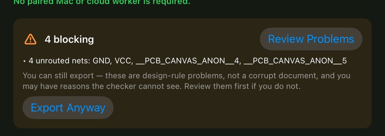
The warning names the affected nets and explains the consequence. Review Problems goes back to the list; Export Anyway proceeds with the board as it stands. 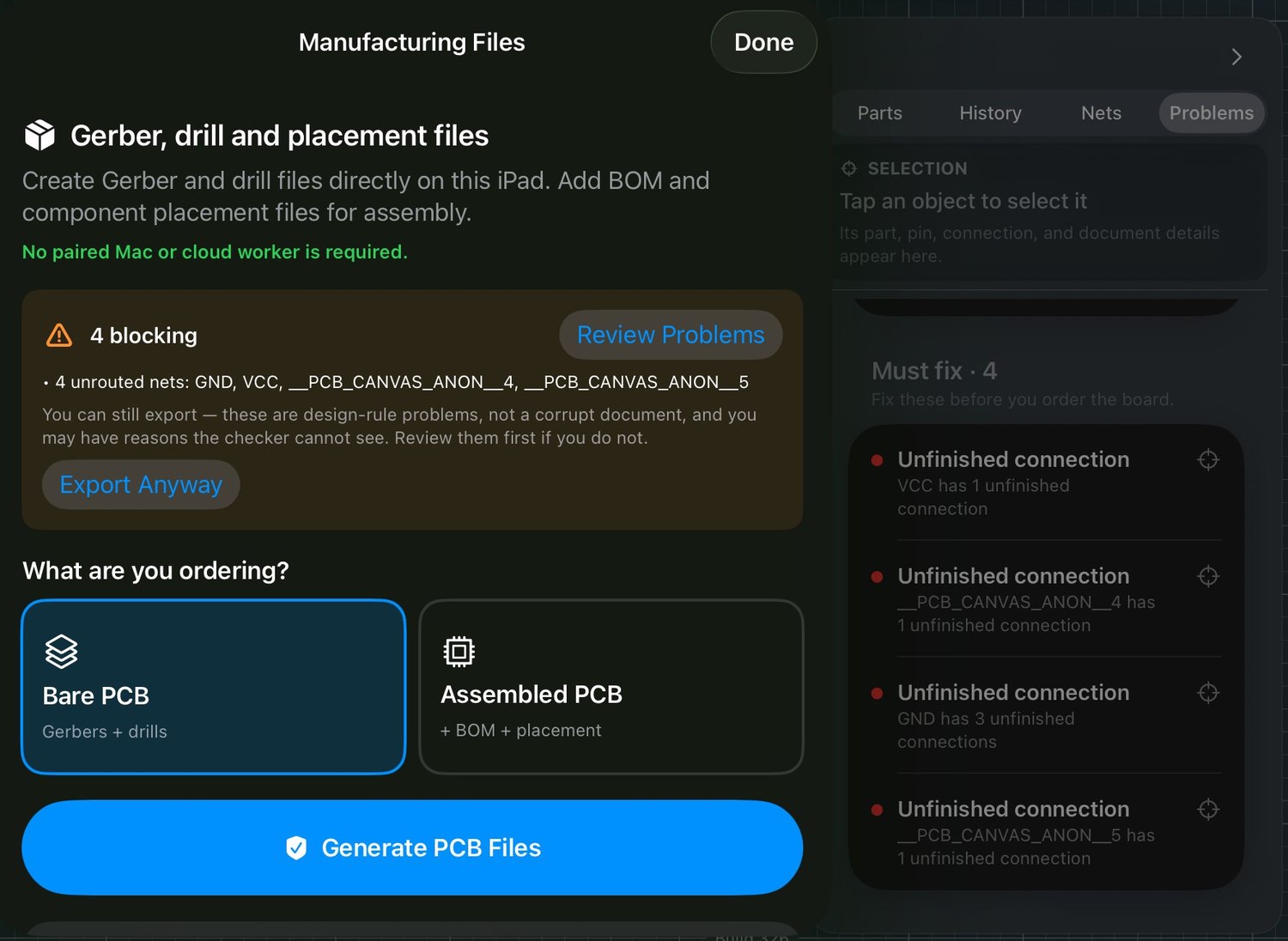
Bare PCB produces Gerbers (one file per copper, mask and silk layer) plus drill files. Assembled PCB adds the BOM, with LCSC part numbers, and the placement file an assembly machine uses to position parts. Files are generated and verified on the iPad: outline closed, drills checked, no paired computer involved. The ZIP can be uploaded to a board house as-is.